Summary of SUNY Polytechnic Creates 3-in-1 Device That Can Be A Diode, A MOSFET And A BJT
Researchers at SUNY Polytechnic Institute developed a single reconfigurable semiconductor device that functions as a p-n diode, MOSFET, and bipolar junction transistor (BJT). This innovation addresses the limitations of Moore's Law by integrating three distinct components into one unit using 2-D tungsten diselenide. The team also created a novel doping technique to achieve ambipolar conduction in this new material, enhancing efficiency and functionality beyond traditional scaling methods.
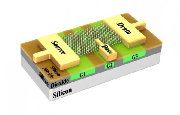
Parts used in the Reconfigurable Semiconductor Device:
- 2-D tungsten diselenide (WSe2)
- Reconfigurable device structure
- New doping method
- p-n diode function
- MOSFET function
- Bipolar junction transistor (BJT) function
In a recently published study, a team of researchers at SUNY Polytechnic Institute in Albany, New York, has suggested that combining multiple functions in a single semiconductor device can significantly improve device’s functionality and efficiency.
Nowadays, the semiconductor industry is striving to scale down the device dimensions in order to fit more transistors onto a computer chip and thus improve the speed and efficiency of the devices. According to Moore’s law, the number of transistors on a computer chip cannot exponentially increase forever. For this reason, scientists are trying to find other ways to improve semiconductor technologies.
To demonstrate the new technology which can be an alternative to Moore’s law, the researchers of SUNY Polytechnic designed and fabricated a reconfigurable device that can be a p-n diode (which functions as a rectifier), a MOSFET (for switching), and a bipolar junction transistor (or BJT, for current amplification). Though these three devices can be fabricated individually in modern semiconductor fabrication plants, it often becomes very complex if they are to be combined.
Ji Ung Lee at the SUNY Polytechnic Institute said,
We are able to demonstrate the three most important semiconductor devices (p-n diode, MOSFET, and BJT) using a single reconfigurable device. We can form a single device that can perform the functions of all three devices.
The multitasking device is made of 2-D tungsten diselenide (WSe2), a new transition metal dichalcogenide semiconductor. This class of materials is special as the bandgap is tunable by varying the thickness of the material. It is a direct bandgap while in single layer form.
Another challenge was to find a suitable doping technique as WSe2 lacks one being a new material. So, to integrate multiple functions into a single device, the researchers developed a completely new doping method. By doping, the researchers could obtain properties such as ambipolar conduction, which is the ability to conduct both electrons and holes under different conditions. Lee said,
Read more: SUNY Polytechnic Creates 3-in-1 Device That Can Be A Diode, A MOSFET And A BJT
- What is the main goal of combining multiple functions in a single semiconductor device?
To significantly improve the device's functionality and efficiency. - Why are scientists looking for alternatives to Moore's law?
The number of transistors on a computer chip cannot exponentially increase forever. - Which three devices can be formed using the single reconfigurable device?
A p-n diode, a MOSFET, and a bipolar junction transistor. - What material is used to make the multitasking device?
2-D tungsten diselenide (WSe2). - How does the bandgap of WSe2 change?
It is tunable by varying the thickness of the material. - What challenge did researchers face regarding WSe2?
WSe2 lacks a suitable existing doping technique. - What property was obtained by developing a new doping method?
Ambipolar conduction, which allows conducting both electrons and holes. - Can these three devices be fabricated individually in modern plants?
Yes, though combining them is often very complex.