Summary of Another ATMEGA4808 Development Board
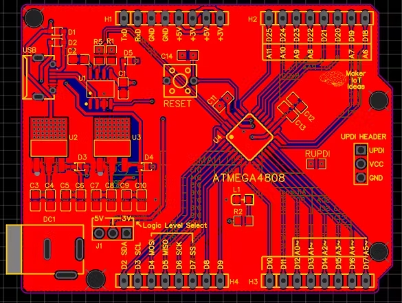
The author redesigned an ATMEGA4808 development board to address flaws in existing clones, adopting the Arduino Uno footprint. Key improvements include dual LDO regulators, a DC barrel jack for 7-12V input, and a jumper for switching between 3.3V and 5V logic levels. While the form factor is cosmetic, enhanced silkscreen labeling aids usability. The project faced supply chain challenges with sensitive USB connectors and non-functional CH340N chips from unreliable vendors, though PCBWay handled manufacturing effectively.
Parts used in the ATMEGA4808 Development Board:
- ATMEGA4808 Microprocessor
- Additional LDO voltage regulator
- DC barrel jack
- Dedicated LDO voltage regulators (two units)
- Micro USB B connector
- CH340N USB to Serial chip
- Soldering stencil
Another ATMEGA4808 Development Board turned out looking very well but highlighted some issues with supply and sourcing of components.
Story
ATMEGA4808 – An Improvement on my previous design? Or Not…
When I first started playing around with the ATMEGA4808, I was impressed as well as disappointed by the Arduino Every “Clone” that I got online. Impressed with the Microprocessor, but disappointed in the way the development board worked, the lack of documentation etc.
I set out to change that by doing my own version, something that I do quite a lot. If I don’t like something, and it is in my ability to create/design my own version, minus any of the perceived(in my opinion mostly) flaws of the original design, I usually do just that.
With that mindset firmly in place, a few weeks ago, I did indeed redesign an ATMEGA4804-based development module, and it worked flawlessly…
As time went by, that little irritating voice in my head got louder and louder… add this, change that, what if it was like this etc.… Many makers will know exactly which little voice I am talking about.
So what did I change?
The short answer to that is a lot. the long and detailed, well let’s see…
- Added an additional LDO voltage regulator, to provide more current.
- A DC barrel jack was included, enabling us to power this from 7v to 12vDC
- Changeable logic level ( switching entire board between 3.3v and 5v operation )with a single jumper.
- Improved labelling of GPIO functions (on the back of the PCB), listing alternative functions etc for each GPIO
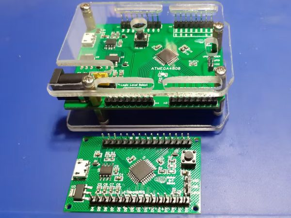
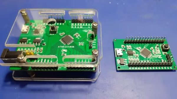
- Put all that into the standard Arduino Uno Footprint…
So, did any of that really matter?
Once again, two answers, one long, one short… so here goes…The added DC barrel jack, with the two dedicated LDO voltage regulators, adds flexibility to power the device externally, opening up possibilities to use it in a stand-alone project, not only on the bench.
The Logic level switching, which at the time, seemed like a very very good idea, now no longer seems so important…Using the Arduino Uno footprint, yeah, so what, it is a neat layout, but apart from using a somewhat ” traditional” footprint, is only cosmetic…
That leaves only the updated silkscreen on the back of the PCB, as well as better labelling on the front…
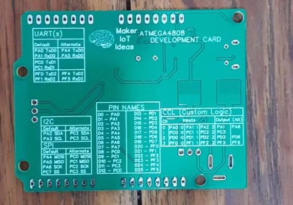
As far as information goes, yes, this is a great help. It will definitely save some time reading datasheets and looking up other stuff…
Does this mean the project was a failure?
Definitely not. I am not negative, but instead, have a tongue-in-the-cheek attitude about how sidetracked I became. I mean, this is basically the exact same board, with just a different form factor. So, in that case, think about it in the context of an Arduino UNO and Arduino NANO. Both of them use the exact same processor but only differ in footprint. ( as well as a few other cosmetic things and functions – the nano having additional analog inputs etc.).\
I am sure that the new form factor will appeal to some, and others will feel it was a completely unneeded design.
The Schematic
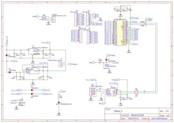
The schematic does not contain any surprises. everything is basically similar to my initial breakout module design, with the exception of the power section. I tried something different, and the jury is still out on how well it actually worked. When powered from USB, the 3.3v LDO Voltage regulator gets fed directly from the USB Voltage, through a protection diode of course.. Similarly, when powering the device using the DC power jack, both LDO regulators are once again fed separately… for the time being, it seems to work well. Time will tell if it was the correct way to do things.
PCB Design
A lot of care was taken to attempt routing of all tracks at the shortest distance possible, as well as using differential pairs for the UART, SPI and I2C peripherals. PCB heatsinks for the LDO regulators, as well as ground planes on both side of the PCB, was also implemented.
Manufacturing
I choose PCBWay for my PCB manufacturing. Why? What makes them different from the rest? PCBWay‘s business goal is to be the most professional PCB manufacturer for prototyping and low-volume production work in the world. With more than a decade in the business, they are committed to meeting the needs of their customers from different industries in terms of quality, delivery, cost-effectiveness and any other demanding requests.
As one of the most experienced PCB manufacturers and SMT Assemblers in China. They pride themselves to be our (the Makers) best business partners, as well as good friends in every aspect of our PCB manufacturing needs. They strive to make our R&D work easy and hassle-free. How do they do that? PCBWay is NOT a broker. That means that they do all manufacturing and assembly themselves, cutting out all the middlemen, and saving us money. PCBWay’s online quoting system gives a very detailed and accurate picture of all costs upfront, including components and assembly costs. This saves a lot of time and hassle.
PCBWay gives you one-on-one customer support, that answers you in 5 minutes ( from the Website chat ), or by email within a few hours ( from your personal account manager). Issues are really resolved very quickly, not that there are many anyway, but, as we are all human, it is nice to know that when a gremlin rears its head, you have someone to talk to that will do his/her best to resolve your issue as soon as possible.
Assembly
The assembly of the ATMEGA4808 development card, as I named the creation, can be done entirely with a standard soldering iron and steady hands, but I chose to order a stencil with the PCB and reflow the PCB on a hotplate.
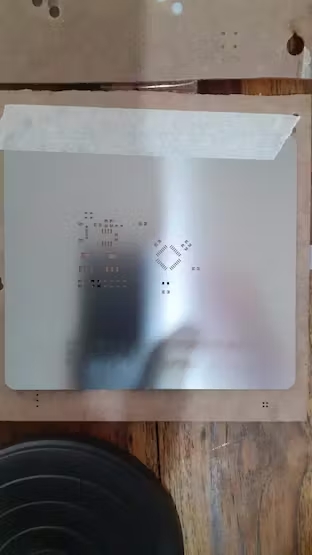
I prefer this way of assembly, as it is generally faster, looks neater, and ultimately uses less solder paste. This particular build did however give me a few headaches, which may be the underlying reason for my tongue-in-the-cheek attitude towards this PCB…
Let us take a look at some of the issues that I encountered. The Micro USB B connector that I used, seems to be quite sensitive to heat. I have a few different batches of these, and some are good, while others are just terrible. ( this happens because I did not buy them all from a reputable supplier, but opted for an online supplier instead – NOT LCSC as I normally do). This resulted in having to change USB connectors a few times. The second issue was the CH340N USB to Serial chip. Due to availability issues, I was once again forced to use an online supplier, and ended up receiving only two working chips out of a batch of 20! The fact that they were super cheap, with super fast shipping should have alerted me that something was wrong…
Source: Another ATMEGA4808 Development Board
- How can I power this board externally?
The DC barrel jack enables powering the device from 7v to 12vDC. - Can I switch the logic level on the board?
Yes, a single jumper allows switching the entire board between 3.3v and 5v operation. - What components are included for voltage regulation?
The design includes two dedicated LDO voltage regulators to provide more current. - Does the new design use the standard Arduino Uno footprint?
Yes, the author put all features into the standard Arduino Uno Footprint. - Why did the assembly process cause headaches?
Issues arose because some Micro USB B connectors were sensitive to heat and many CH340N chips were defective. - Which manufacturer did the author choose for PCB production?
The author chose PCBWay for their professional prototyping and low-volume production services. - How does the author prefer to assemble the board?
The author prefers using a stencil and reflowing the PCB on a hotplate for speed and neatness. - What information is now available on the PCB back?
The back of the PCB lists alternative functions for each GPIO to improve labeling.