Summary of ATMEGA328P Microcontroller
The ATmega328P is an 8-bit CMOS microcontroller featuring a RISC CPU, auto-sleep modes, and an internal temperature sensor. It supports multiple communication protocols including UART, SPI, and I2C, along with digital I/O, timers, ADC channels, and PWM capabilities. Widely used in embedded systems and Arduino projects, it offers versatile programming methods and internal protections for various engineering applications.
Parts used in the ATmega328P Microcontroller:
- Digital Input/Output Pins (PORTB, PORTC, PORTD)
- Interrupt Pins (IN0, IN1)
- USART Communication Module (RX, TX, XCK)
- SPI Communication Module (MOSI, MISO, SS, SCK)
- I2C Communication Module (SDA, SCL)
- Timers Modules (T0, T1, TOSC1, TOSC2, ICP1)
- System Clock Pin (CLKO)
- Comparator Module (AN0, AN1)
- Capture/Compare/PWM Channels (OC0B, OC0A, OC1A, OC1B, OC2A, OC2B)
- Analog to Digital Converter Channels (ADC0-ADC5, AVCC)
- Analog Reference Pin (AREF)
- Reset Pin
- Power Pins (VCC, GND)
- Oscillator Pins (XTAL1, XTAL2)
ATmega328P is one of the high performances AVR technology microcontroller with a large number of pins and features. It is designed by 8-bit CMOS technology and RSIC CPU which enhance its performance and its power efficiency get improved by auto sleeps and internal temperature sensor. This ATmega328P IC comes with internal protections and multiple programming methods which helps the engineers to priorities this controller for different situations. The IC allows multiple modern era communications methods for other modules and microcontrollers itself, which is why the microcontroller ATmega328P usage has been increasing every day.
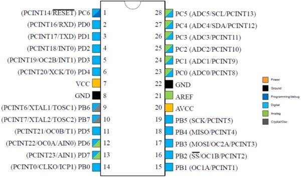
Pinout Diagram ATmega328P
In this section, we will see the usage of each pin and pin diagram details for this 28 pin microcontroller. This picture shows the pinout diagram:
Othe alternative options for ATMEL microcontrollers are ATtiny45, ATtiny88, ATtiny85
Pin configuration Details
DIGITAL INPUT/OUTPUT PINS
This microcontroller has three digital ports (B, C, D) such as PORTB, PORTC, and PORTD. All these pins can be used as digital input/output. On top of that, each port can be used for other purposes. To use them as output/input or for any other function it should be defined first otherwise there won’t be any default function by all I/O pins. Digital I/O pins of the controller are:
- PB0 – GPIO14
- PB1 – GPIO15
- PB2 – GPIO16
- PB3 – GPIO17
- PB4 – GPIO18
- PB5 – GPIO19
- PB6 – GPIO9
- PB7 – GPIO10
- PC0 – GPIO23
- PC1 – GPIO24
- PC2 – GPIO25
- PC3 – GPIO26
- PC4 – GPIO27
- PC5 – GPIO28
- PC6 – GPIO1
- PD0 – GPIO2
- PD1 – GPIO3
- PD2 – GPIO4
- PD3 – GPIO5
- PD4 – GPIO6
- PD5 – GPIO11
- PD6 – GPIO12
- PD7 – GPIO13
INTERRUPT PINS
Most of the electrical functions required an interrupt system to operate like AC dimmer, etc. ATmega328P gives the support of 2 interrupts within the controller which can be used to get the attention of the CPU at any instant. Interrupt pins of ATmega328P are given below:
- IN0 – GPIO4
- IN1 – GPIO5
ATmega328P UART Communication Module
Although there are multiple kinds of communication systems within the devices and modules but the most common one is USART. It is one of the simplest and easiest method for implement and understanding by most of the developers and systems. In this method, two wires used to send and receive the data. The USART pins of microcontroller ATmega328P are:
- RX – GPIO2
- TX – GPIO3
The data can be sent by specified the sending rate within the controllers but it can also use the external clock pin to keep the data sync.
- XCK – GPIO6
USART/UART communication system ca be used to program the microcontroller.
SPI Communication ATmega328P
It one of the best serial communication systems in the case of multiple peripherals. SPI protocol allows multiple devices to use the same channel for communication. It consists of four wires, two for data sending and one for clock but the fourth wire is used to select the peripherals knows as a select slave. In the case of multiple peripherals number of the select slave, pins will be increased. The SPI pins of the microcontroller are:
- MOSI – GPIO17
- MISO – GPIO18
- SS – GPIO16
- SCK – GPIO19
I2C Communication Module
Most of the peripherals come with the I2C communication method which is one way at a specific time. I2C protocol only uses one data wire and one clock wire. Data wire will transfer and receive the data and clock wire will send the clock pulse to keep the data sync. The wires on the microcontroller are:
- SDA – GPIO27
- SCL – GPIO28
TIMERS MODULES
ATtiny328P has two internal timers. We can use these timers to make counters and to generate pulses. Both of these timers are dependent on an oscillator. Both timers can use the internal and external clock to operate, but they also have an internal pin which can be used to count according to the external pulses. All of these pins in microcontroller ATmega328P are given below:
- T0 – GPIO6
- T1 – GPIO11
- TOSC1 – GPIO9
- TOSC2 – GPIO10
- ICP1 – GPIO
ICP1 is an input capture pin which can be used to capture the external pulse at a specific interval of time. When an input pulse will occur on this pin then it will generate a timestamp which can tell when the external signal was received.
SYSTEM CLOCK
The internal clock and external clock pulses can be divided by the Prescaler and their value can be received at an external pin. The external pin for divided clock pulses will be:
- CLKO – GPIO14
COMPARATOR MODULE
The microcontroller has internal comparator modules for analog signal. This module takes the input in inverting and non-inverting form which can be used further for any internal purpose or it can also be used to generate the output signals. Comparator pins of the microcontroller are listed below:
- AN0 (Positive) – GPIO12
- AN1 (Negative) – GPIO13
ATmega328P CAPTURE/COMPARE/PWM Channels
There are six capture/compare/PWM pins are used to generate the desired time pulse-based signal. It uses a Prescaler to divide the time pulse. All of these pins in ATmega328P are:
- OC0B – GPIO11
- OC0A – GPIO12
- OC1A – GPIO15
- OC1B – GPIO16
- OC2A – GPIO17
- OC2B – GPIO5
ANALOG TO DIGITAL CONVERTER Channels
In ATmega328P there are 6 ADC channels that can be used to convert the analog signal to digital. The analog converter needs to be activated first by its power pin (AVCC). The ADC channels use power supply voltage as a reference to differentiate the different levels of the analog signal. The analog pins of the controller are:
- ADC0 – GPIO23
- ADC1 – GPIO24
- ADC2 – GPIO25
- ADC3 – GPIO26
- ADC4 – GPIO27
- ADC5 – GPIO28
- AVCC – Pin20
AREF PINS
Sometimes the analog signal voltages are fluctuating but it kept measuring by the controller according to the power input of the controller. To measure it by any other power input or by the power of analog signal generating device, an analog voltage reference AREF will be used. This pin will detect the maximum value of the analog signal and then it will be able to give the proper output. AREF pin in ATmega328P is:
- AREF – GPIO21
RESET: In ATmega328 there is some reset to restart the microcontroller in some conditions. In all of these resets there is an external reset to reset the device using an external signal:
- RESET – GPIO1
POWER: Every controller needs the power to operate and it always has a power input pin. In ATmega328P the power pins are three in number. One pin is for voltage and the remaining two are for common ground. Both of these ground pins are connected internally, it doesn’t matter which one is used. The power pins of the microcontroller are:
- VCC – Pin7
- GND – Pin8, Pin22
OSCILLATOR: The controller comes with 8MHz changeable oscillator. However, it can also use the external oscillator up to 40MHz. To use the external oscillator, oscillation pins will be required for input and output of the signal. Those pins are given below:
- XTAL1 – GPIO9
- XTAL2 – GPIO10
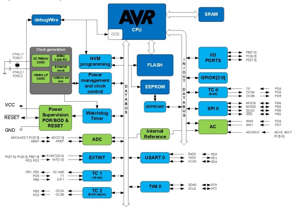
ATMEGA328P Block Diagram
The block diagram of the microcontroller ATmega328P is given below:
Pin Mapping of ATmega328P with Arduino
ATmega328 comes in Arduino, which helps the users to code the program in Arduino instead of assembly or other controller languages. Arduino is popular because of its vast online data and high-level language, and this helps the developer to code the controller program in Arduino and them convert it into the microcontroller code. In case of Arduino the pin configuration for the controller will be the following:
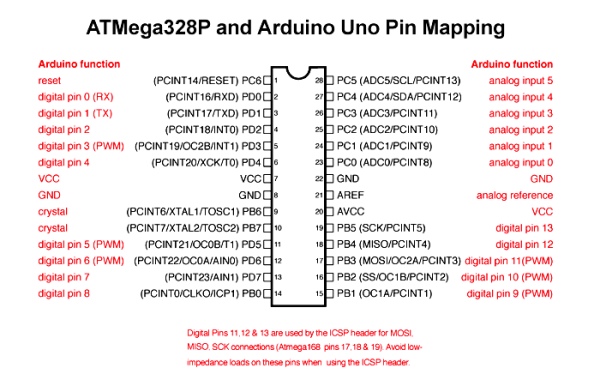
In the case of Arduino, the pins become specific to their functionality. During using the compiler of ATmega328 almost all pins can be used as GPIO. However, during the usage of Arduino, each pin will perform the specific function only, but the controller will still be able to perform all the operations like ATmega328.
APPLICATIONS
- Most of the embedded systems like IoT based uses ATmega328 to perform multiple kinds of operations due to its vast examples and helping material on the internet.
- It is used in Arduino which makes it the most popular controller.
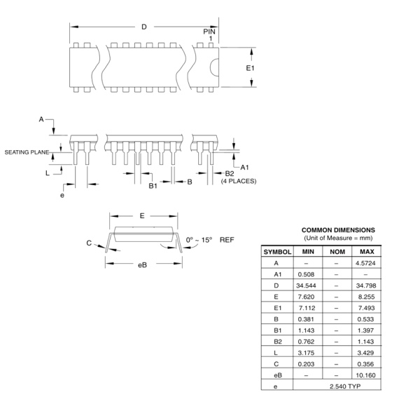
2D DIAGRAM
Source: ATMEGA328P Microcontroller
- What technology does the ATmega328P use?
It is designed using 8-bit CMOS technology and features a RISC CPU. - How many digital ports are available on this microcontroller?
This microcontroller has three digital ports named PORTB, PORTC, and PORTD. - Can the ATmega328P support interrupt systems?
Yes, the controller gives support of 2 interrupts which can be used to get the attention of the CPU at any instant. - Which communication method uses two wires to send and receive data?
The USART method is one of the simplest ways where two wires are used to send and receive the data. - How many wires does the SPI protocol consist of?
The SPI protocol consists of four wires, two for data sending, one for clock, and one for selecting peripherals. - Does the I2C protocol use separate wires for data and clock?
Yes, the I2C protocol only uses one data wire and one clock wire. - How many internal timers does the ATmega328P have?
The text states that the ATtiny328P has two internal timers, though the context implies these features apply to the series. - What is the function of the AREF pin?
The AREF pin detects the maximum value of the analog signal to measure it by any other power input or device. - Can the external oscillator frequency go up to 40MHz?
Yes, while it comes with an 8MHz changeable oscillator, it can also use an external oscillator up to 40MHz. - Why is the ATmega328P popular among developers?
It is popular because it is used in Arduino, which allows coding in high-level languages instead of assembly.