
Summary of AVR ADC using ATmega16 with TLC549 Serial ADC in Proteus Simulation
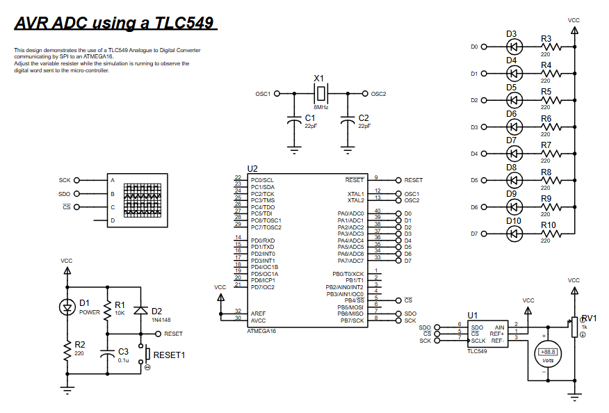
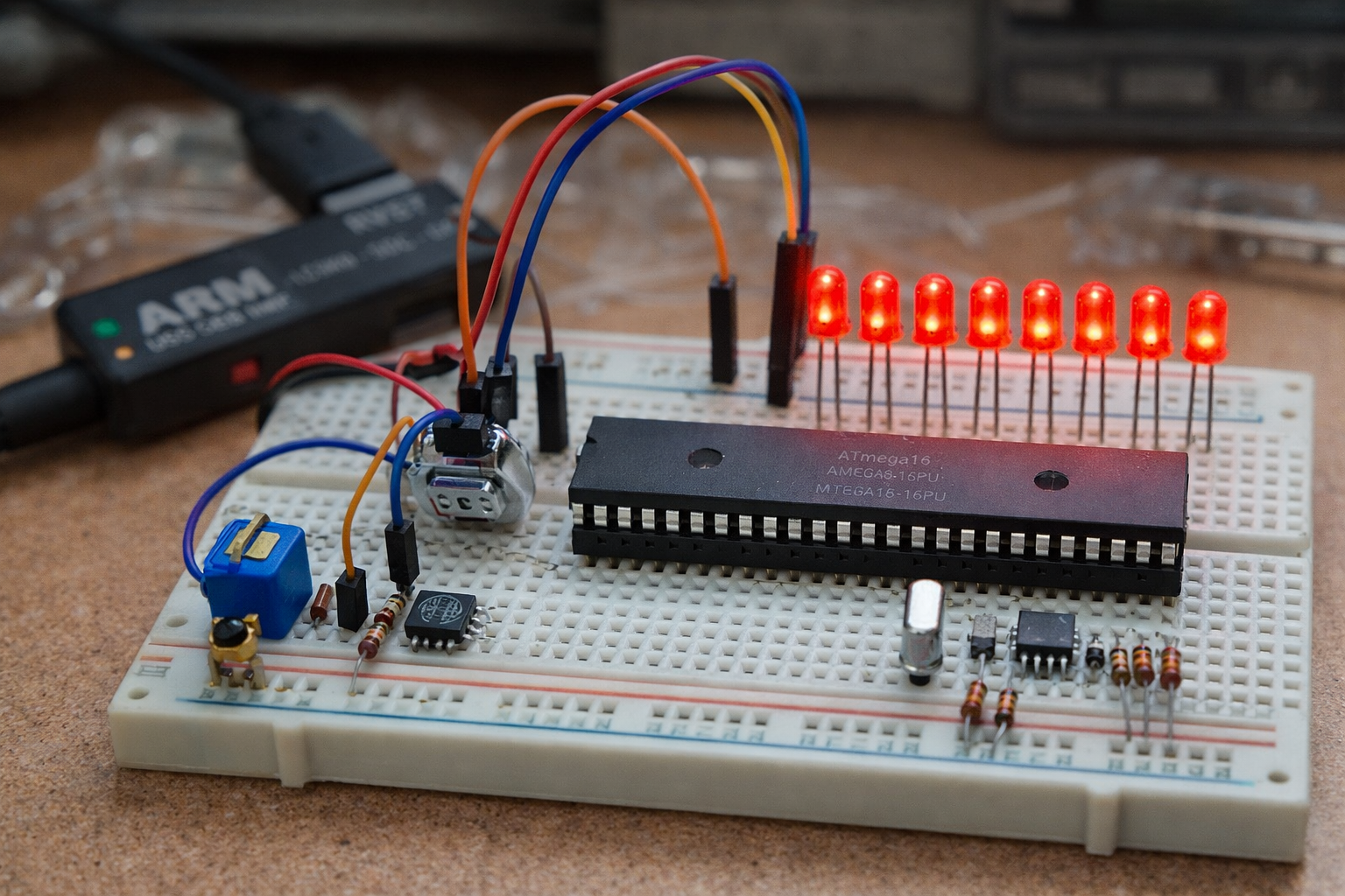
AVR ADC using TLC549 demonstrates interfacing a TLC549 8-bit serial ADC to an ATmega16 via SPI in a Proteus VSM simulation. A potentiometer provides analog input; the TLC549 converts it to 8-bit data, sent over SPI to the ATmega16, which inverts the byte and outputs it on PORTA to drive eight LEDs. The project illustrates SPI communication, external ADC interfacing, and real-time analog monitoring for learning and prototyping.
Parts used in the AVR ADC using TLC549:
- ATmega16 microcontroller
- TLC549 8-bit serial ADC
- 8 MHz crystal oscillator
- 22pF capacitors for crystal stabilization
- Potentiometer (RV1)
- Eight LEDs
- Resistors for LED current limiting
- Reset switch
- Diode 1N4148 for reset circuit protection
Introduction
AVR ADC using TLC549 demonstrates how analog signals from sensors can be converted and processed by a microcontroller. Analog signals from sensors cannot be processed directly by most microcontrollers because they operate using digital logic. To bridge this gap, Analog-to-Digital Converters (ADC) are used in many microcontroller projects and embedded systems.
This project demonstrates an AVR-based ADC interface using the TLC549 serial ADC with an ATmega16 microcontroller. The design is simulated in Proteus, allowing users to observe how analog input values are converted into digital data and displayed via LEDs.
The project is ideal for learning SPI communication, external ADC interfacing, and practical embedded systems development. By adjusting the variable resistor in the simulation, users can observe real-time digital outputs representing the analog signal.
How the Project Works (Overview)
The system reads an analog voltage using the TLC549 8-bit serial ADC and sends the digital result to the ATmega16 microcontroller through SPI communication.
Here is the working sequence:
-
The analog input voltage is generated using a variable resistor (potentiometer).
-
This voltage is fed into the TLC549 ADC.
-
The TLC549 converts the analog signal into 8-bit digital data.
-
The ATmega16 communicates with the TLC549 using SPI (Serial Peripheral Interface).
-
The microcontroller reads the ADC data via SPI.
-
The received data is inverted in firmware and sent to PORTA.
-
Eight LEDs connected to PORTA display the digital value.
Changing the potentiometer value alters the analog voltage, which results in a different digital output displayed on the LEDs.
Workflow Explanation
The circuit can be divided into several functional blocks:
Analog Input Stage
A potentiometer (RV1) provides a variable voltage source that acts as the analog signal input to the TLC549 ADC.
ADC Conversion Block
The TLC549 converts the analog voltage into an 8-bit digital value. This device communicates with the microcontroller using a serial interface compatible with SPI.
Microcontroller Processing Unit
The ATmega16 receives digital data from the ADC using SPI communication. The firmware processes the data and sends the result to output pins.
Output Display Block
Eight LEDs connected to PORTA (PA0–PA7) display the converted digital value.
Clock and Reset Circuit
An 8 MHz crystal oscillator provides the system clock, while the reset circuit ensures proper initialization during power-up.
Key Features
-
External TLC549 serial ADC interface
-
SPI communication between ADC and ATmega16
-
Real-time analog voltage monitoring
-
8-bit digital output display using LEDs
-
Designed and tested in Proteus VSM simulation
-
Demonstrates embedded systems ADC interfacing
-
Adjustable analog input using a potentiometer
Components Used
| Component | Description |
|---|---|
| ATmega16 | AVR microcontroller |
| TLC549 | 8-bit serial ADC |
| Crystal Oscillator | 8 MHz clock source |
| Capacitors | 22pF for crystal stabilization |
| Potentiometer (RV1) | Variable analog voltage source |
| LEDs (8x) | Digital output indicators |
| Resistors | Current limiting for LEDs |
| Reset Switch | Microcontroller reset |
| Diode (1N4148) | Reset circuit protection |
Applications
This type of ADC interface microcontroller project can be used in many practical applications:
-
Sensor data acquisition systems
-
Embedded monitoring devices
-
Digital voltmeters
-
Temperature or light monitoring systems
-
Industrial measurement systems
-
Educational embedded systems labs
Explanation of Code
The firmware is written using AVR-GCC and compiled with WinAVR.
Port Initialization
PORTA is configured as an output port. The ADC digital values will be displayed on LEDs connected to these pins.
SPI Configuration
The ATmega16 SPI module is initialized in Master Mode with a clock frequency of Fosc/128. The microcontroller generates clock pulses to communicate with the TLC549 ADC.
Chip Select Control
The CS (Chip Select) line enables communication with the ADC. When CS is low, the TLC549 sends digital data through the SPI data line.
Data Acquisition
The microcontroller initiates an SPI transfer. The TLC549 returns the 8-bit converted digital value.
Output Processing
The received data is inverted and written to PORTA so the LED pattern reflects the digital value.
Source Code
/********************************
FILE NAME:        S_AD.c
CHIP TYPE:        ATMEGA16
CLOCK FREQUENCY:  8MHZ
IDE:              VSMStudio
COMPILER:         AVR-GCC
TIME:             September 2010
********************************/
#include <avr/io.h>
#include <util/delay.h>


#define uchar unsigned char
#define uint unsigned intProteus Simulation
The Proteus VSM simulation demonstrates how the ATmega16 reads analog data from the TLC549 ADC.
Simulation behavior:
-
The potentiometer adjusts the analog voltage input
-
TLC549 converts this voltage into 8-bit digital data
-
ATmega16 reads the data through SPI communication
-
The resulting digital value appears as LED patterns
As the potentiometer rotates, the LED pattern changes to reflect the new digital value.
Conclusion
This project demonstrates a practical AVR microcontroller project using the TLC549 ADC with SPI communication. By simulating the design in Proteus, developers can clearly observe how analog signals are converted and processed by a microcontroller.
It provides an excellent hands-on introduction to ADC interfacing, SPI communication, and embedded systems design, making it a valuable learning project for students and DIY electronics enthusiasts.
Complete File
AVR ADC using ATmega16 with TLC549 Serial ADC in Proteus Simulation
- How does the analog input get generated?
A potentiometer (RV1) provides a variable voltage that serves as the analog input. - How is the analog voltage converted to digital?
The TLC549 ADC converts the analog voltage into an 8-bit digital value. - How does the ATmega16 receive ADC data?
The ATmega16 receives the 8-bit ADC data via SPI communication. - What is done with the received ADC data in firmware?
The received data is inverted in firmware and written to PORTA. - How is the digital value displayed?
Eight LEDs connected to PORTA (PA0–PA7) display the inverted digital value. - What clock source is used for the system?
An 8 MHz crystal oscillator provides the system clock. - How is the TLC549 enabled for communication?
The CS chip select line is pulled low to enable the TLC549 to send data over SPI. - What development tools are mentioned for the firmware?
The firmware is written using AVR-GCC and compiled with WinAVR.
