Summary of Analyzing the vintage 8008 processor from die photos
The article celebrates the 45th anniversary of the Intel 8008 microprocessor by reverse-engineering its unique on-chip stack circuits. Unlike modern designs using RAM, the 8008 employs shift-register counters to generate pseudo-random values for its stack, saving gates. The piece traces this design back to the Datapoint 2200 terminal, which used slow shift-register memory and separate i3101 RAM chips for its stack, leading to an architecture where the program counter resides at the top of the stack.
Parts used in the Intel 8008:
- 18 external wires
- 3500 tiny transistors
- Metal wiring layer
- Data bus
- Shift-register counters
- On-chip stack
The revolutionary Intel 8008 microprocessor is 45 years old today (March 13, 2017), so I figured it’s time for a blog post on reverse-engineering its internal circuits. One of the interesting things about old computers is how they implemented things in unexpected ways, and the 8008 is no exception. Compared to modern architectures, one unusual feature of the 8008 is it had an on-chip stack for subroutine calls, rather than storing the stack in RAM. And instead of using normal binary counters for the stack, the 8008 saved a few gates by using shift-register counters that generated pseudo-random values. In this article, I reverse-engineer these circuits from die photos and explain how they work.
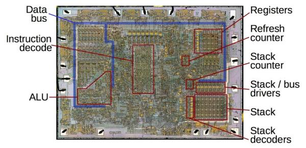
The image below shows the 8008’s tiny silicon die, highly magnified. Around the outside of the die, you can see the 18 wires connecting the die to the chip’s external pins. The 8008’s circuitry is built from about 3500 tiny transistors (yellow) connected by a metal wiring layer (white). This article will focus on the stack circuits on the right side of the chip and how they interact with the data bus (blue).
For the 8008 processor’s birthday, I’m using the date of its first public announcement, an article in Electronics on March 13, 1972 entitled “8-bit parallel processor offered on a single chip.” This article described the 8008 as a complete central processing unit for use in “intelligent terminals” and stated that chips were available at $200 each.1
You might think that an intelligent terminal is a curiously specific application for the 8008 processor. There’s an interesting story behind that, going back to the roots of the chip: the Datapoint 2200 “programmable terminal”, introduced in June 1970. The popular Datapoint 2200 was essentially a desktop minicomputer with its processor consisting of a board full of simple TTL chips. The photo below shows the CPU board from the Datapoint 2200. The chips are gates, flip flops, decoders, and so forth, combined to build a processor, since microprocessors didn’t exist at the time.
Processors typically use a stack to store addresses for subroutine calls, so they can “pop” the return address off the stack. This stack is usually stored in main memory. However, the Datapoint 2200 used slow shift-register memory2 instead of expensive RAM for its main storage, so implementing a stack in main memory would be slow and inconvenient. Instead, the Datapoint 2200’s stack was stored in four i3101 RAM chips, providing a small stack of 16 entries. 3 4 The i3101 was Intel’s very first product, and held just 64 bits. In the photo above, you can see the chips in their distinctive white packaging each with a large “i” for Intel. 5
To keep track of the top of the stack, the Datapoint 2200 used a 4-bit up/down counter chip to hold the stack pointer. The clever thing about this design is there’s no separate program counter (PC) and stack; the PC is simply the value at the top of the stack. You don’t need to explicitly push and pop the PC onto the stack; for a subroutine call you just update the counter and write the subroutine address to the stack.
Read more: Analyzing the vintage 8008 processor from die photos
- How many transistors does the 8008 contain?
The circuitry is built from about 3500 tiny transistors. - Where is the stack stored in the 8008 compared to modern architectures?
The 8008 has an on-chip stack rather than storing the stack in RAM. - What type of counters does the 8008 use for the stack?
The processor uses shift-register counters that generate pseudo-random values instead of normal binary counters. - Why did the original Datapoint 2200 store the stack in RAM instead of main memory?
The Datapoint 2200 used slow shift-register memory for main storage, making a stack in main memory slow and inconvenient. - Which specific RAM chips were used in the Datapoint 2200 for the stack?
The system used four i3101 RAM chips to provide a small stack of 16 entries. - What was the capacity of the i3101 chip used in the Datapoint 2200?
The i3101 held just 64 bits. - How does the Datapoint 2200 handle the program counter without a separate register?
The program counter is simply the value at the top of the stack, eliminating the need for a separate program counter. - When was the Intel 8008 first publicly announced?
The chip was first announced in an article in Electronics on March 13, 1972.