Summary of GLASGOW INTERFACE EXPLORER IS A HARDWARE DEBUGGING TOOL FOR DIGITAL ELECTRONICS
The Glasgow Interface Explorer is an open-source multi-tool for digital electronics, powered by a Lattice Semi iCE40 FPGA. Designed for developers and hobbyists, it enables hassle-free communication with various digital devices without needing extra components. It features high-speed USB connectivity, programmable GPIO banks with voltage regulation and ADC sensing, flexible GPIOs with level shifters, differential I/O pairs, LEDs, and ESD protection, making it a versatile hardware debugging solution.
Parts used in the Glasgow Interface Explorer:
- Lattice Semi iCE40 HX8K FPGA
- USB-C port connected to FX2 high-speed USB interface
- Two 8-channel GPIO banks
- Programmable linear voltage regulator (1.8 – 5V)
- Sense ADC for voltage and current monitoring
- 16 flexible GPIOs with level shifters
- Independent software-controlled 10K Ohm pull-up/down resistors
- ESD protection diodes
- 14x differential pair I/O
- User-controlled LEDs
- Status LEDs
- Dedicated SYNC connector
1BitSquared has launched a crowdfunding campaign for a highly capable and extremely flexible open source multi-tool called Glasgow Interface Explorer.
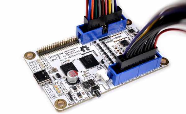
Glasgow Interface Explorer for digital electronics is powered by Lattice Semi iCE40 FPGA and created for hardware developers, electronics hobbyists, engineers, tinkerers, and
anyone else who wants to communicate with a wide selection of digital devices with minimum hassle.
The board aims to offer a broad selection of capabilities with more than “some wires and, depending on the device under test, external power.” You can attach it to devices without any need for extra active or passive components.
Some of its Key Features and Specifications include:
- iCE40HX8K Lattice Semiconductor FPGA
- 1x USB-C port connected to FX2 high-speed USB interface; 480 Mbps throughput
- 2x 8-channel GPIO banks, each with:
- A dedicated programmable linear voltage regulator, configurable from 1.8 – 5V with up to 150 mA of power
- A dedicated sense ADC capable of monitoring the GPIO bank voltage and current, with interrupt trigger thresholds that can be set
- 16 highly flexible GPIOs, each with:
- A peak frequency of 100MHz
- A dedicated level shifter with individual direction control, and,
- An independent, software-controlled 10K Ohm resistor Pull-Up/-Down resistor
- ESD protection diodes for all GPIOs
- Set of 14x differential pair I/O, connected directly to the FPGA (optional); can be used for high speed interfaces
- Up to 5x User-controlled LEDs
- Up to 5x Status LEDs, and,
- 1x Dedicated SYNC connector
Read more: GLASGOW INTERFACE EXPLORER IS A HARDWARE DEBUGGING TOOL FOR DIGITAL ELECTRONICS
- What is the Glasgow Interface Explorer?
It is an open source multi-tool for digital electronics powered by a Lattice Semi iCE40 FPGA. - Who is this board created for?
It is created for hardware developers, electronics hobbyists, engineers, tinkerers, and anyone wanting to communicate with digital devices. - Does the board require extra active or passive components to attach to devices?
No, you can attach it to devices without any need for extra active or passive components. - How fast is the USB interface on the board?
The board has a USB-C port connected to an FX2 high-speed USB interface with 480 Mbps throughput. - Can the GPIO banks be configured for different voltages?
Yes, each bank has a dedicated programmable linear voltage regulator configurable from 1.8 to 5V. - What is the peak frequency of the flexible GPIOs?
The 16 highly flexible GPIOs have a peak frequency of 100MHz. - Does the device include protection against electrostatic discharge?
Yes, there are ESD protection diodes for all GPIOs. - Are there options for high speed interfaces?
Yes, there is a set of 14x differential pair I/O connected directly to the FPGA for high speed interfaces.