Summary of Microcontroller Based Interface Design
This article details the third installment of a "System Interface Design" series, focusing on creating a resource map (Interface Control Document) for an autonomous rover. It explains how to allocate ATmega328P I/O pins between the Arduino Duemilanove and an Adafruit Motor Shield to manage DC motors, stepper motors, IR sensors, and a digital gyro. The project aims to enable spatial awareness for autonomous navigation across varied terrain without human intervention.
Parts used in the Autonomous Rover Project:
- ATmega328P microcontroller
- Arduino Duemilanove board
- Adafruit Motor Shield
- DC motors
- Bipolar stepper motor
- IR Sensors
- Digital gyro
- L293D H-Bridge ICs
- 74HC595 serial-to-parallel integrated circuit
Introduction
The third installment in the “System Interface Design” series guides you through the process of crafting the resource map, which is a crucial component in Part 1, and the allocation of resources for sensors and actuators (including a Long Range IR sensor) in Part 2.
Until now, the Resource Map has been presented as if it simply materialized like magic. However, when you’re employed by a company as a system engineer, it will be your responsibility to generate the resource map, technically termed an Interface Control Document (ICD). This ICD serves as a directive for the subsystems (such as mechanical engineering, command and data handling, power, etc.) that collectively form the system design, which in this context pertains to the rover.
1.Mission Objective
The primary objective of this project is to create a robot with spatial awareness. The robot will use this awareness to autonomously navigate a course featuring 4-6 terrain features placed at varying distances from its initial landing site. The success of the project hinges on the robot’s ability to reach these target locations without human intervention, employing an intelligent design approach. While this goal may seem deceptively simple, it entails three distinct phases of development, transforming the robot from a standard RC vehicle into a sophisticated project. This document outlines the specific steps required to elevate our platform to this advanced level. For more detailed information on the rover’s requirements, please refer to the Mission Plan.
As previously mentioned, we will employ a combination of sensors to provide our robot with what we refer to as “robo-vision.” This “robo-vision” involves the integration of (2) IR Sensors and a digital gyro. These components will work in unison to enable the robot to precisely determine its position in relation to the surrounding target locations, allowing it to reach these objectives autonomously. (Let’s remain optimistic about this.)
2. System Design
Mapping of Microcontroller Resources
One of the key responsibilities of a systems engineer involves resource allocation, and in the context of a spacecraft, these resources are limited and encompass factors such as mass and power. In the case of our rover, another limited resource to consider is the available number of I/O pins on the ATmega328P microcontroller. Tables 2.1 and 2.2 serve as a mapping of these I/O pins to the various sensors, actuators, and associated interface electronic module signals required to construct the reference design. The allocation of I/O pins is visually indicated by a change in row color, shifting from light orange to white. In simpler terms, once a row appears white, it signifies that the I/O pin has been utilized. In the upcoming section, we will delve into the creation of each column and explore how our I/O pin resources have been distributed.
Column 1 – ATmega 328 I/O Pins
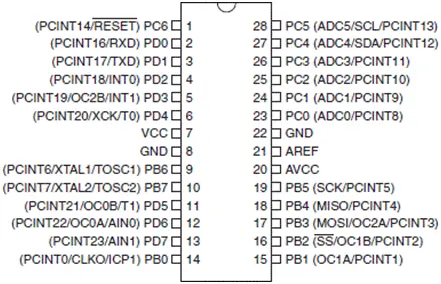
In Figure 2.1, you can observe the ATmega328P housed within a 28-pin Dual In-line Package (DIP). You can locate Figure 2.1 within the ATmega328P Datasheet (hint: consider checking page 2). When inspecting each pin in this figure, you’ll notice that the majority of them are assigned to the three general-purpose I/O ports (PB7..PB0, PC6..PC0, and PD7..PD0). These general-purpose I/O pins serve multiple functions by being multiplexed with various ATmega328P peripheral subsystems. For instance, the pins used for the Universal Synchronous and Asynchronous Serial Receiver and Transmitter (USART) peripheral subsystem, such as the transmit (TXD) and receive (RXD) interface pins, are shared with the general-purpose I/O pins PD1 and PD0, respectively.
Moreover, these pins can also be utilized to detect changes in the input state of a pin, as indicated by PCINT17 and PCINT16. This function is referred to as a Pin Change Interrupt (PCINT).
For our rover’s sensors and actuators to connect to the ATmega328P, we need to arrange all these I/O pins within column 1.
If that information isn’t sufficient, you should also be aware that these pins can serve the purpose of identifying alterations in the input status of a pin, specifically PCINT17 and PCINT16, and this is referred to as a Pin Change Interrupt (PCINT).
To connect our rover’s sensors and actuators to the ATmega328P, we will need to arrange all these I/O pins in the first column.
Column 2 – Arduino Header Pins
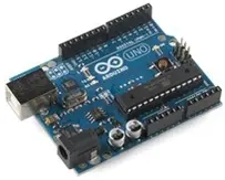
At the heart of the Arduino Duemilanove lies the ATmega328P microcontroller. This Arduino Duemilanove is a cost-effective, open-source computing platform built around a straightforward I/O board and a freely available Integrated Development Environment (IDE).
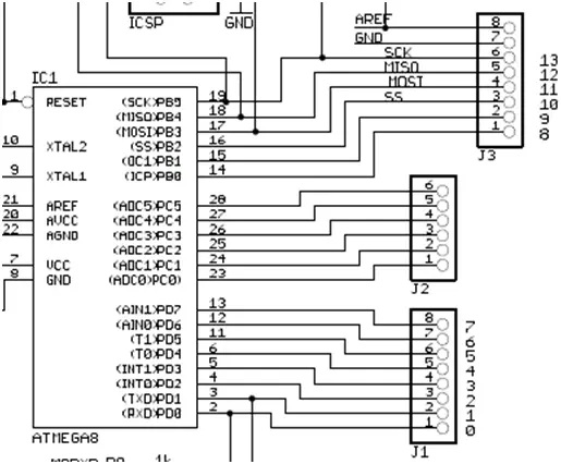
The series of connectors visible on the upper and lower edges in Figure 2.2 are linked to the I/O pins of the ATmega328P IC, which is situated near the lower right section of the board. Regrettably, the Arduino board employs an entirely different naming scheme for these I/O pins, as demonstrated in Figure 2.3. This figure is a segment of the Arduino Duemilanove Eagle Schematic, and it aids in mapping the ATmega328P IC pins to their corresponding connectors on the Arduino. As an example, our USART TXD and RXD pins are linked to header J1 pins 2 and 1, designated as Digital 1 and 0 (it’s important to acknowledge that this can be somewhat perplexing).
The second column in the table establishes the mapping of Arduino Duemilanove pins to their respective pins on the ATMEL ATmega328P, as presented in the first column. The illustration below is an excerpt extracted from the Arduino Duemilanove Eagle Schematic.
Here are some design notes to consider:
– Pins 1 to 6 on J2 are denoted as “Analog In” and correspond to pins 0 to 5 on the board.
– When you examine your Arduino Duemilanove board, you’ll notice that certain digital pins are labeled as PWM (Pulse Width Modulation), specifically 3, 5, 6, 9, 10, and 11.
Column 3 – Adafruit Motor Shield
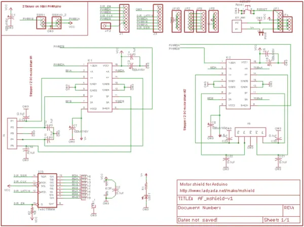
In the reference design, we are adopting the Adafruit Motor Shield. In Figure 2.4, you can observe the Motor Shield, often referred to as a daughter board, seamlessly inserted into the Arduino Duemilanove Board, which is commonly termed a mother board. This Motor Shield plays a pivotal role by supplying the necessary logic and drivers to facilitate the setup and energization of the DC motors and Bipolar stepper motor employed in our reference design. Furthermore, we will establish connections between our IR sensors and digital gyro with the Motor Shield.
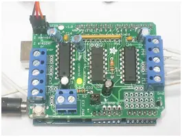
You can access the Eagle CAD PCB layout and schematic files via the provided links. To open these files on your laptop, you will need to download Eagle CAD, and we’ll be using the free version. For your reference, I’ve included the schematic of the Adafruit motor shield as depicted in Figure 2.0.
In Table 2.1, Column 3 presents in tabular format the Adafruit motor shield pin names assigned to both the Atmega328P and Arduino Duemilanove. It would have been more convenient if a uniform naming convention had been adopted. These names encompass signals connected to the integrated circuits (ICs) on the motor shield and signals linked to headers designated for our sensors.
Column 3 also introduces a set of new pins (X1-P5..P2, X2-P5..P2) that aren’t directly associated with either the Atmega328P or Arduino. Internally, these pins are connected to two L293D H-Bridges, a topic covered in the DC and stepper motor labs. Externally, these screw connectors will be employed for wiring our DC motors (Column 6 and 7) and stepper motor (Column 8).
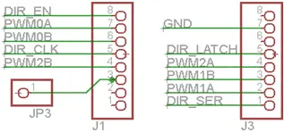
Now, let’s delve into the ATmega328P I/O resources utilized by the motor shield. To map these resources (pins) onto the Motor Shield, I’ve extracted from the Motor Shield schematic (Figure 2.5) the segment illustrating how Arduino headers J1 and J3 (as indicated in Column 2) are linked to the Digital Input Register (DIR) and Pulse Width Modulation (PWM) integrated circuits (ICs) on the Motor Shield (refer to Columns 4 and 5). These ICs are identified as IC1, IC2, and IC3 on the schematic.
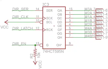
Column 4 – Adafruit Digital Input Register (DIR)
Column 4 specifies the ATmega328P pin resources (as listed in Column 1) designated by Adafruit for the Digital Input Register (DIR) on the motor shield. These signals are denoted by the “DIR” prefix in Column 3. The DIR is realized using a 74HC595 serial-to-parallel integrated circuit (IC). Communication between the ATmega328P and the DIR is achieved through the Serial Peripheral Interface (SPI) protocol, which is software-implemented. Unfortunately, this situation is not ideal because the ATmega328P features a hardware implementation of the SPI, connected to a different set of pins, rendering it unusable in this context.
Column 5 – Pulse Width Modulation (PWM)
The ATmega328P is equipped with three timer subsystems, denoted as T0, T1, and T2. Within each of these timer subsystems, you’ll find two compare registers, labeled as A and B. These six compare circuits’ outputs can be harnessed to produce Pulse Width Modulated (PWM) signals, and they are connected to I/O pins with the names PWM0A, PWM0B, PWM1A, PWM1B, PWM2A, and PWM2B.
In the context of the Adafruit motor shield, PWM0A, PWM0B, PWM2A, and PWM2B are linked to two L293D H-Bridge integrated circuits (ICs). As for PWM1A and PWM1B, they remain available for rovers that incorporate one or two servos or can be utilized as general-purpose I/O pins. If your design doesn’t involve servos, you have the flexibility to include these pins in the pool of available pins for your sensors.
PWM control of DC Motors
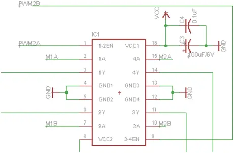
Once more, Figure 2.7, excerpted from the motor shield schematic, reveals the interconnection of ATmega328P wires from the two comparator circuits of Timer 2 (PWM2A and PWM2B) to the control inputs of one of the L293D H-Bridge integrated circuits. In alignment with Figure 2.7, the configuration inputs M1A, M1B, M2A, and M2B are derived from the DIR registers as shown in Figure 2.6. Further insights into H-Bridges will be provided in the motor labs.
Source: Microcontroller Based Interface Design
- What is the primary objective of this rover project?
The main goal is to create a robot with spatial awareness that can autonomously navigate a course featuring 4-6 terrain features without human intervention. - How does the robot achieve robo-vision?
It uses a combination of two IR sensors and a digital gyro to determine its position relative to target locations. - Which microcontroller is central to this system design?
The project utilizes the ATmega328P microcontroller housed within an Arduino Duemilanove. - What component provides logic and drivers for the motors?
The Adafruit Motor Shield supplies the necessary logic and drivers for DC motors and the bipolar stepper motor. - How are the DIR signals realized on the motor shield?
The Digital Input Register is realized using a 74HC595 serial-to-parallel integrated circuit communicating via a software-implemented SPI protocol. - Can PWM1A and PWM1B be used for other purposes?
Yes, these pins remain available for servos or general-purpose I/O if the design does not involve them for motor control. - What technical term is used for the resource map generated by the systems engineer?
The resource map is technically termed an Interface Control Document or ICD. - Why is the hardware SPI unusable on the ATmega328P for the DIR register?
The hardware SPI is connected to a different set of pins than those required by the motor shield's DIR interface.