Summary of NFC Transmitter and Receiver Using Atmega1284
This article details the construction of a custom Near Field Communication (NFC) module using two ATmega1284p microcontrollers. The system employs resonant inductive coupling at 13.56MHz, utilizing coupled coils as antennas. A local oscillator generates the carrier frequency, which modulates digital messages from the transmitter. The receiver uses a unity-gain amplifier and hysteresis comparator to restore the signal before processing it via serial port. The project emphasizes building the wireless transmission mechanism from scratch to understand radio frequency procedures rather than creating a complex application.
Parts used in the NFC Module Project:
- ATMega1284p Microcontroller
- DIP Socket
- Pin Header
- NPN 2N3904 Transistor
- Custom PC Board
- RS232 Connector
- LM358 Comparator
- MAX4233 Serial Connector
- Solder Board
- 13.56MHz Crystal Oscillator
- 74LS00N NAND Gates
Introduction
Our project is building one set of NFC module including a NFC transmitter and a NFC receiver both using ATmega1284p microcontroller. We will be using coupled coils to transmit message modulated by a high frequency carrier, whose frequency is the standard frequency for Near Field Communication (NFC) – 13.56MHz (Wikipedia, 2013).
In our project, we build a local oscillator which generates the accurate NFC carrier by using the crystal oscillator circuit. To set up the near field wireless transmission, we build two coupled coils as antennas to transmit and receive the message, which is the application of resonant inductive coupling. These two coils are tuned to resonate at the frequency of 13.56MHz. We use one ATmega1284p microcontroller to generate the message and modulate it with the carrier from our local oscillator. The modulated high-frequency signal will be transmitted through the coupled coils to the receiver including a transistor amplifier, a hysteresis comparator and another ATmega1284p microcontroller which processes the received signal and displays it through serial port.
As opposed to many colleagues who make complicated design with very dedicated application, we choose to dive into the working procedure of the wireless module and build it from scratch. The goal of our project is not a very detailed application, but a basic method of transmitting message through wireless channel which can be utilized by a large amount of applications. Through this project, we hope to make ourselves clearer about the working procedure of transmitting message at radio frequency and improve our practical skills.
High Level Design
Background
Near Field Communication (NFC) is a new technology that has emerged in the past decade. It is a set of standards for smartphones and similar devices to establish radio communication with each other by touching them together or bringing them into close proximity, usually no more than a few inches. This idea was originally used by radio-frequency identification, or RFID. RFID allows a reader to send radio waves to a passive electronic tag for identification, authentication and tracking. NFC, inherited from the working scheme of RFID, is only capable for a short range communicating and thus inherent secure data exchange can be applied. Many individuals and companies have seen the great potential of this new technology and thus many applications have been developed. For example, a company named Log-IC has used NFC tags to keep track of thermometer readings of temperature sensitive goods. Google also developed Google Wallet using mobile NFC. Currently, integration of NFC technology into mobile phones has been proved a practical solution. This creates a potentially huge market for NFC applications because nowadays almost everyone has a cellphone. All those novel NFC products are interesting and its promising future motivates us to figure out the pros and cons of this technology. Thus, we decided to build our own NFC module which can be used for extensive applications in the future.
Overview
In our design, we intended to use LC tank to work as antenna. Since the standard working frequency for NFC transmitter is 13.56MHz, the LC product is required to be very small. It turns out that the self-tuned inductor (coil) has the resonant frequency of 13.56MHz. We build our own 13.56MHz oscillator to work as the carrier frequency. The digital message from ATmega1284p is modulated by the carrier frequency and then transmitted through the wireless channel. Because of the loss during the transmission, the voltage of the received signal is not high enough to trigger comparator. To solve this problem, we build a unity-gain amplifier whose output is low voltage for input 1 with high frequency signal and high voltage for input zero. Then we use inverting comparator with hysteresis whose output signal is 5V for digital 1 and 0V for digital 0. Output from the amplifier is inverted after the comparator and hence the original digital message is restored. Then this restored digital signal is processed in ATmega1284 and the message is displayed through serial port.
Logical Structure
1. Hardware
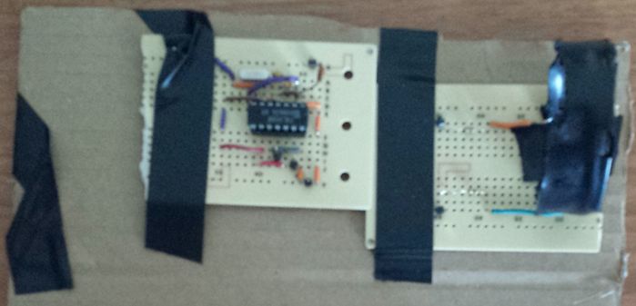
The hardware of this project is composed of two main parts, transmitter and receiver. Transmitter block includes user interface (ATmega1284p), local oscillator (13.56MHz carrier generator) and antenna (LC Tank). Receiver block includes antenna, demodulation and ADC Circuit (unity gain amplifier and hysteresis comparator with inverting-input) and signal processing (ATmega1284p).
2. Software
We will be using USART1 on ATmega1284p microcontroller to transmit and receive messages. To transmit a message, we first put it into a transmit buffer which will be sent through TX1 (PD3) one character at a time. For reception, hardware USART will automatically read bits from RX1 (PD2) and put it into UDR1 (USART Data Register). All we need to do is just read from this register and put it into a receive buffer which be further processed later.
3. Hardware and Software Tradeoff
The first tradeoff we have is the processing of the received signal. Since our transmission is achieved at a high frequency (13.56MHz), the loss during the transmission is relatively high. The voltage of received signal is quite low (around 300mV). Converting this low amplitude, high frequency signal into digital signal is really tricky. If the demodulation and ADC tasks are done by the microcontroller, more complex software processing method is required. This rapidly increases the computation burden of the microprocessor. However, if we use some hardware to share tasks of signal processing, the workload of the microprocessor will be reduced. Also, the signal is easily converted to desired digital signal by using our circuit implantation. Details about the implementation are described in the latter section.
4. Related Standards
In our project, the transmission frequency we use is 13.56MHz. It is within the band of 13.110 and 14.110 MHz. Thus, it is regulated by FCC 15.209 and FCC 15.229.
(a) The field strength of any emissions within the band 13.553-13.567 MHz shall not exceed 15,848 microvolts/meter at 30 meters.
(b) Within the bands 13.410-13.553 MHz and 13.567-13.710 MHz, the field strength of any emissions shall not exceed 334 microvolts/meter at 30 meters.
(c) Within the bands 13.110-13.410 MHz and 13.710-14.010 MHz the field strength of any emissions shall not exceed 106 microvolts/meter at 30 meters.
(d) The field strength of any emissions appearing outside of the 13.110-14.010 MHz band shall not exceed the general radiated emission limits in § 15.209.
(e) The frequency tolerance of the carrier signal shall be maintained within ±0.01% of the operating frequency over a temperature variation of −20 degrees to 50 degrees C at normal supply voltage, and for a variation in the primary supply voltage from 85% to 115% of the rated supply voltage at a temperature of 20 degrees C. For battery operated equipment, the equipment tests shall be performed using a new battery.
(f) In the case of radio frequency powered tags designed to operate with a device authorized under this section, the tag may be approved with the device or be considered as a separate device subject to its own authorization. Powered tags approved with a device under a single application shall be labeled with the same identification number as the device.
Table 1 FCC Regulations
|
Frequency(MHz) |
Field Strength(microvolts/meter) |
Measurement distance(meters) |
|
0.009-0.490 |
2400/F/(kHz) |
300 |
|
0.490-1.705 |
24000/F/(kHz) |
30 |
|
1.707-30 |
30 |
30 |
Since our project is just building a prototype of NFC Module not for commercial use, the following standards are not required here (http://www.waazaa.org/download/), but for further application development, these standards must be taken into consideration.
Near Field Communication has a standard working frequency of 13.56MHz and for 13.56MHz air interface communication, ISO/IEC 18000-3 is required.
NFC standards cover communications protocols and data exchange formats, and are based on existing radio-frequency identification (RFID) standards including ISO/IEC 14443 and FeliCa. The standards include ISO/IEC 18092 and those defined by the NFC Forum, which was founded in 2004 by Nokia, Philips Semiconductors and Sony.
5. Existing Patent and Copyright
For our oscillator design, we used the design idea from the website of Home of the Z80 CPU. We modified the design to work at 13.56MHz for our project. Also, we modified the comparator design from Cornell University ECE4760 Lab4.We changed it into an inverting hysteresis comparator with different reference voltage.
Hardware Design
Coil Antenna
The antenna is built using two coils. The wireless transmission between these two blocks is done using resonant inductive coupling. A coil with oscillating current will generate an oscillating magnetic field. Other coil nearby will be driven by the oscillating magnetic field and hence signal will be transmitted.
Since our transmission is done at a high frequency, the parasitic capacitance takes a huge effect. A real coil can be approximately modeled as shown in Figure 2. Cp is the parasitic capacitance and R is resistance under DC voltage.
Figure 2 LC Tank Circuit
The resonant frequency given by this RLC model is . While, it is very hard to control the value of the parasitic capacitance (resistance can be ignored for long distance coil). The method we used here is measuring the self-resonant frequency of the coil and then adjust the size of the coil accordingly. After picking the coil with a certain inductance, we measure its self-resonant frequency. If this frequency is lower than 13.56MHz, we need to scale down the size of the coil. The inductance of a coil is given by the equation where D = coil diameter in inches, N = Number of turns, l = coil length in inches. So the inductance of the coil becomes smaller if we reduce the number of turns of the coil. Also, reducing the turns of the coil will decrease the parasitic capacitance as well since the parasitic capacitance is from the individual wire turn of the coil. If the picked coil has a self-resonant frequency higher than 13.56MHz, a capacitance () can be added in parallel with the coil to increase the resonant frequency. We assume the resonant frequency after adding is and for . By using this two sets of data we can find the value of L and Cp.(If you want to make it more precise, you can measure a third set of data to find value of R). For our own experience, after reducing the coil size for three times, we happened to get a coil with a approximate self-resonant frequency of 13.56MHz. One thing to mention here consider the transmitting efficiency will be affected by inductance. The maximum achievable efficiency is , where , , , , and are the Q facor of the transmitter and receiver coils. After some math, we can obtain approximately, If we deduce the inductance by cutting turns, which will make Q smaller and hence the efficiency will become lower.
Carrier Frequency Generation
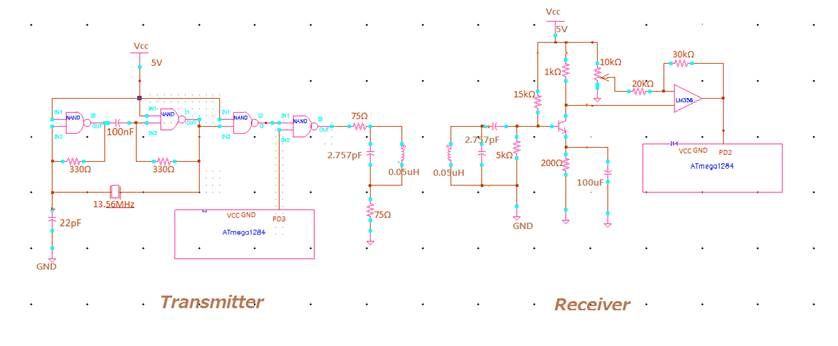
Before a digital message being transmitted through wireless channel, it must be modulated to a higher frequency which is more suitable for wireless transmitting. ATmega1284 is running at a frequency 16MHz and its actual frequency upper bound is a lot lower. We cannot use MCU to generate a 13.56MHz signal so an oscillator is required. Our oscillator is a modified design from Home of the Z80 CPU, the schematic is shown in the red block in Figure 3. Basic idea to build an oscillator is an amplifier with a feedback network. In order for an oscillator to operate, two conditions must be satisfied: a. the loop power gain must be equal to unity; b. the loop phase shit must be equal to 0, 2pi, 4pi, etc. The exact frequency at which an oscillator will operate is dependent on the loop phase angle shifts within the oscillator circuit. The most common method to provide a stable net phase shift is to use a quartz crystal unit in the feedback loop. Figure 3 shows a depcition of the rectacne vs. frequency of a quartz crystal unit. As we can see from the plot, a quartz will have two frequencies of zero phase fs and fa. fs is referred as the series resonant frequeny and the higher one, fa, is reffered as the parallel frequency. At the seris resonant point, the resistnace is minimal and the current flow is maximal. At the prallel reonant point, the resistance is maximal and the current flow is minimal. Therefore, the parallel resonant frequency should never be used as the controlling frequency of an oscillator circuit. Thus, we choose a series reonsant osicllator cirucit design as shown in Figure 4. The two resitors are used to bias the invertor and the invertor will operate at its linear region. The resistor also provides a negative feedback to the invertor. The 100nF capacitor is used to block DC voltage. The 22pF capacitor is used to bias the crystal at high frequecny. We choose these values so that the series resonant oscialltor will operate at the natural frequency of the crystal, which is 13.56MHz.
Parts List:
|
Part |
Description |
Quantity |
Unite Price |
Total Price |
Supplier |
|
ATMega1284p |
MCU |
2 |
5 |
10 |
Bruce Land |
|
DIP Socket |
For MCU, NAND Gates, Op-amp |
3 |
0.5 |
1.5 |
Bruce Land |
|
Pin Header |
Connections within each board and between different blocks |
74 |
0.05 |
3.7 |
Bruce Land |
|
NPN 2N3904 |
Unity-gain Amplifier |
1 |
0.2 |
0.2 |
Bruce Land |
|
Custom PC board |
MCU board |
2 |
4 |
8 |
Bruce Land |
|
RS232 connector for custom PC board |
Serial Connector for PC board |
2 |
1 |
2 |
Bruce Land |
|
LM358 |
Comparator |
1 |
0.5 |
0.5 |
Bruce Land |
|
MAX4233 for custom PC board |
Serial Connector for PC board |
2 |
7 |
14 |
Bruce Land |
|
Solder Board |
For transmitter and receiver board |
4 |
2.5 |
10 |
Bruce Land |
|
13.56MHz crystal |
For oscillator design |
1 |
0.56 |
0.56 |
Digikey |
|
74LS00N |
NAND gates for oscillator |
1 |
0.67 |
0.67 |
Bruce Land |
|
Total Cost |
|
|
|
51.13 |
For more detail: NFC Transmitter and Receiver Using Atmega1284
- How is the NFC carrier frequency generated?
A local oscillator circuit using a quartz crystal unit generates the accurate 13.56MHz carrier frequency. - What method is used for wireless message transmission?
The project uses resonant inductive coupling with two coupled coils tuned to resonate at 13.56MHz. - Why is an amplifier needed in the receiver block?
An amplifier is required because voltage loss during transmission results in low received signals that cannot trigger the comparator alone. - Which standard frequency is used for this NFC module?
The system operates at the standard NFC frequency of 13.56MHz. - What happens if the coil self-resonant frequency is lower than 13.56MHz?
The size of the coil must be scaled down by reducing the number of turns to increase the resonant frequency. - How does the receiver restore the original digital message?
The signal passes through a unity-gain amplifier and an inverting hysteresis comparator to convert it back to 5V or 0V digital levels. - Why was hardware chosen over software for demodulation?
Hardware processing reduces the computation burden on the microprocessor caused by the high frequency and low amplitude of the received signal. - What regulations govern the transmission frequency used?
The 13.56MHz frequency falls within the band regulated by FCC 15.209 and FCC 15.229.