Introduction
The goal of this project was to develop a working bench-top microcontroller platform for a shark tag. It is to be used for on-animal, in-situ data logging applications involving sharks and potentially other large pelagics.
For this project I used the Atmel Mega32 microcontroller to develop the core platform and functionality of a data archival tag. The tasks ranged from logging sensor data to developing a simple user interface that requires only the addition of a laptop and a custom RS232 serial cable in the field. I used an off-the-shelf SD (Secure Digital) card using flash memory for large capacity multi-read/write data storage. The microcontrollers ADCs (analog to digital converters) were used to convert analog voltages produced by select sensors into digital format. These digital sensor values are then sent to the SD card by the microcontroller for storage using a rudimentary SPI (Serial Peripheral Interface) communication protocol. The user is able to download the recorded data from the tag to a computer via an RS232 serial link using hyperterminal or the serial communication utility of their choice. This data is recalled from flash by the tag and sent to hyperterminal in a 1 x n matrix that is easily parsed in MATLab. In essence, my tag platform is a data logger with a simple interface that allows the user to prepare it for deployment and to download data upon recovery. Ultimately, this tag is a tool to be used by scientists, engineers, or any variety of field technician.
Rationale
When I was seven my grandfather gave me a National Geographic VHS on sharks. Since then I have harbored a mild obsession with sharks and strove to learn all that I can about these fascinating yet poorly understood creatures of the ocean. My interest has matured into a desire to build tools for helping scientists to better study these animals. Building my own shark tag is the consummate dovetailing of my interests in engineering and sharks. As this is a microprocessor design course, the focus of this project is on the design of a microprocessor based tag platform that can be developed into an ocean ready tag at a later date.
Being an engineer and having had the opportunity to work with sharks and whales in a scientific capacity, I developed a strong interest in the engineering of technology used to humanely study ocean life. The purpose of tagging an animal in the wild is to collect data for the purposes of biology, ecology, or conservation that cannot be made by direct observation. I have some specific ideas on improving current methods and science, and feel developing my own tag via the ECE 476 final project was a great place to get started.
Logical Structure/Function
This project is a mlange of work done in hardware and software. The main functional elements of this project are the logging of sensor data to flash memory, and the user interface. The logging and storage of data must be robust, and the user interface must be simple, easy to understand, and prevent the user from doing something they dont want to do (like accidentally erasing data from a tag before it has been downloaded). The data logging aspect has three main components: the sensors, the analog to digital converter (ADC), and the flash memory. The user interface is primarily a menu system accessed via hyperterminal that allows the user to prepare the tag for deployment and to download data acquired during a deployment.
A sensor on the tag works by measuring some environmental property and producing a calibrated analog voltage that is correlated to the actual property under measurement (pressure, temperature, etc). My tag platform can work with any sensor that has an analog or digital output within the range of 0-5V. A temperature and pressure sensor were used for this project. However, for this stage of development, my sensor choice was really immaterial and more to illustrate overall platform functionality. One of the ideas is to make a portable platform that can be adapted for whatever sensor a scientist has an interest in using. Any sensor actually used in a tag must be seriously vetted for hydrostatic pressure compliance as animals tagged in the ocean can at times dive to significant depths that cause certain components to fail. This type of evaluation takes weeks of pressure cycling components under load, not to mention a pressure test facility.
Continuing on, the analog voltages produced by the sensors are read by the ADC and converted to either an 8 or 10 bit (depending on the needed resolution) digital value. The Mega32 sports eight 10bit ADCs, three of which were used for this project. Once a digital voltage is acquired, it is stored in a 512 byte data buffer on the microcontroller. When the buffer is full, its contents are written to memory and the buffer is cleared and filled up again with sensor data. This continues ad infinitum until the data logging mode of the tag is arrested by an LOW command on the RESET pin. For storage I used flash memory in the form of a SD/MMC card. While these cards have a sophisticated data communication protocol that allows them to be used by high-tech electronics such a digital cameras and computers, they also support a simple SPI protocol that is used by many microcontrollers including the Mega32. The memory architecture of an SD card is divided into groups, which are divided into sectors, which are divided into blocks composed of 512 bytes. The nature of these cards is such that memory must be written in discrete 512 byte/block chunks. Any data sent outside of a 512 byte block will not be saved and will cause an error in the write command. All information relating to memory allocation or user defined settings are stored in the Mega32s EEPROM, and neither settings nor data is lost when the tag is powered down.
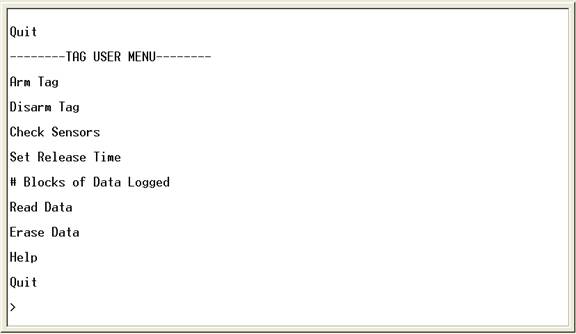
The user interface is essential a menu system that is displayed on a computer screen via a RS232 serial connection and serial communication terminal of preference. It comes up each time the tag is power-up or reset. This includes post deployment power up. Care was taken into providing a forgiving environment that permits the entering of spurious text submissions. The user simply enters the listing/function of the menu that they are interested in, and navigates as prompted by the menu. A picture of the menu can be seen below in Figure 1.
The tag will not record data until it is armed. Once it is armed, it will wait for a saltwater switch to sense that it is in the water (and ideally on an animal). The tag has a blinking LED that indicates that it is in fact armed and waiting to go in the water. When the saltwater switch is tripped, this LED will stop blinking and another LED will blink to indicate that it has entered data logging mode and exited the mode where it is simply armed and waiting. It will then commence logging sensor data. Data logging will continue on until arrested by a reset command, sent by asserting LOW on the RESET pin.
As this is a data archival tag, the tag will need to be recovered in order to retrieve data. Thus, the tag will need some means of releasing from its attachment to the animal. The only tried and tested way of doing releases in the ocean is by using Nichrome burn wire releases. These work by putting a potential across a Nichrome wire in saltwater. The sea water acts as a conductor, and current flows through the NaCl ions in the sea water from the Nichrome wire to an anode. In the process, the Nichrome wire dissolves away. In the menu the user will set the deployment/release time. The tag will not begin counting down to release time until the saltwater switch is tripped and it begins logging data. Upon this time, a voltage will be applied to the Nichrome wire. The tag will not begin counting down to release time until the saltwater switch is tripped.
Once the tag is recovered, the user will exit data logging mode by means of a RESET. This can be done in the field with a 9V battery and two leads connecting to the RESET pin and a ground pin. Once a serial communication application is open, the user can check that data was logged to memory by querying the tag with a # command from the main menu prompt. The user can then read and download the data from the tag via a read command. The data can be logged directly to a text file and imported to MATLab for parsing and post processing.
Hardware
As this project is an element of a larger project which I will hopefully finish developing and actually deploy, in light of the time limitations placed on this project, no efforts were made to package the hardware. Having had experience designing tags from a mechanical end, two of the biggest considerations are size and weight. To achieve satisfactory results for either of these involved numerous trade-offs whose consequences endure and hence require debated and thoughtful consideration. Thus, all hardware was left in a form most conducive to prototyping and modification. An STK500 board was used for ease in programming the Mega32 and for accessing ports for prototyping. A breadboard was used for constructing and prototyping the circuits for the sensors and the SD card. A nice SD card prototyping breakout board bought from www.Sparkfun.com.
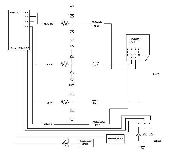
The SD card used requires a 2.7-3.6V supply voltage, and so for convenience an external 3.2 volt regulator was used. The SD card also uses Low Voltage logic levels. As the Mega32 outputs standard 5V TTL logic levels, these levels needed to be regulated down to not damage the SD card. This was done by constructing a simple two diode and one resistor voltage regulator consisting of two forward biased diodes in series that can be seen in Figure 2 and Figure 3. This was done for the Data In, CLK, and Chip Select SPI lines going to the SD card. Although the SD card Data Out line is at a lower voltage level, it was not stepped up as its logical high output is still well within the range of a 5V TTL signal. However, in a final version it may be prudent to step it up as an increased signal will yield a better signal to noise ratio. However, all of this level adjusting could be eliminated by using a Mega32L, which runs half as fast (8MHz) as a Mega32 and has Low Voltage level logic and power requirements. This will almost surely be done as it simplifies design and consumes less power, something critical in tag design. Further, we dont need to sample data that fast and 16MHz is overkill. See Figure 3. for the interface and connections between the Mega32 and the SD card.
The sensors used were an LM34 temperature sensor, and a Freescale MPXM2010GS pressure sensor found kicking around the lab. Their accompanying circuitry was trivial. A non-inverting operational amplifier with a gain of 2 was used for the temperature sensor. As mentioned above, these sensors served as stand-ins for future and undoubtedly more expensive sensors yet to be determined and vetted.
Software
There are two main aspects of software design for the tag. One is the menu system and user serial I/0 interface, and the other are the functions used for tag operation, data logging, and talking to the SD card. All code was embedded C code written and compiled in the CodeVision programming environment. Hyperterminal was used to read out the serial line. It was set for 9600 baud, 8 data bits, no parity, 1 stop bit, and no flow control.
The menu has a forgiving interface that allows for erasing mistyped characters and writes like a normal text editor, unlike the standard serial Hyperterminal interface which requires hitting enter and going to the next line to reenter a mistyped key. It runs a transmitting and received function called tx_rx_loop() which is interrupt driven and fires every time Timer0 overflows, updating the screen with the current buffer values. As Timer0 is an 8bit timer, this occurs every 16e6MHz/256=62500Hz. The menu system is driven by a function called menu() which calls tx_rx_loop() and accepts user input. The user input is sent to a buffer called linein[] and is handled accordingly. The menu itself is essentially a giant case statement/state machine that depending on the user input allows for different functionality. Each case looks simply for the first letter in the buffer linein[], so if a command is typed incorrectly, it still takes the user to the correct destination provide the first letter was correct. This means a lazy person could simply type the first letter of each command to navigate through the menu. The menu allows for arming the tag, downloading data, checking number of full memory blocks, and interrogating the SD card by calling function defined elsewhere in the program designed for specific tasks. Once the called function performs its duty, it is exited and the program returns to the case statement, and thus the main menu prompt. To let the user know that the tag is in fact armed while in menu browsing mode, once armed, the text entered by the user will be sandwiched by right pointing arrows. Once the menu is exited, a flashing LED will continue to let the user know the tag is armed and waiting for deployment and the saltwater switch to be tripped.
The other software for the Mega32 runs the data logging functions and allows for communication with the SD card. This was the most challenging code to write, and despite looking at several examples for similar SPI communication with an SD card, in the end I used such code as a guide and wrote my own. This was the only way to really know what was going on and the only way I was able to get things to work. While all of the functions are important, the most critical first function to get working was a function to initialize the SD card into SPI mode. Doing this correctly required understanding the default behavior of the SD card and what is needed to exit this default behavior. In doing this I became intimately familiar with the SANDISK SD card data sheet. The SPI mode of operation is simple and utilizes only a CLK, chip select (CS), and Data In and Data Out line for communication and data transfer; a subset of the standard SD card data lines. The SPI communication lines were initialized in software by setting B.4 for CS, B.5 for MOSI, B.6 for MISO, and B.7 of the CLK. Also critical is setting up the SPI configuration register where SPCR = 0b01011110 and SPSR = 1.
When powered up, the SD card starts up not in SPI mode but in its normal mode of operation known as bus mode. The SD Card is based on commands and data bit-streams that are initiated by a start bit and terminated by a stop bit. The SPI channel is byte oriented. Every command (sent or received) or data block is built of eight bit bytes and is byte aligned (multiples of eight clocks) to the CS signal. Like the SD Bus protocol, the SPI messages are built from command, response and data-block tokens. Commands like read and write have data transfers associated with them that are sent via tokens that are transmitted MSB first. Upon power up, to enter SPI mode, the CS signal must be asserted negative during the reception of the reset command, CMD0. This is needed to disable what is known as a Cyclic Redundancy Check (CRC) which is intended to protect the SD Card commands, responses and data transfer against transmission errors on the SD Card bus. One CRC is generated for each unique command and is checked for every response on the CMD line. A CRC mismatch forces an error and nullifies any command sent. For data blocks, a CRC is generated for each data line per transferred block. It is necessary to disable CRC checking to enter SPI mode. Since the card powers up in SD Bus mode, one command must be send in this mode, thus CMD0 must be followed by a valid CRC byte or it wont be recognized. Although the card is in bus mode, when starting up and only when starting up the reset command can be sent using SPI. The default command structure/protocol for SPI mode is such that the CRC checking is disabled. To get here we must send a valid CRC command that tells the SD card to disable CRC until further notice and enter SPI mode. The reset command, CMD0, always generates the same 7 bit CRC of 4A(hex). Adding an end bit 1 (basically a bit0 from bit7 making a full byte) creates a complete CRC byte of 95(hex). The complete CMD0 sequence appears as 40 00 00 00 00 95 (hex). Once this command is received, the SD card ignores all new CRC bits and is effectively in SPI mode. Once in SPI mode the card will respond with the SPI R1 response. Reception and examination of this response is critical to knowing if the card is ready and doing what you think it is doing. It sends a unique response for each command. Once in SPI mode, all the communication between host (Mega32) and SD is controlled by the host/master. The host starts every bus transaction by asserting the CS signal low. It should be noted and obvious that every time the card is power cycled, the SD cad must be reinitialized to reenter SPI mode.
While all the SD Card commands are available in SPI mode, utilizing them proved difficult. I believe this was due to timing issues relating to the sending and receiving of data tokens for different commands which I did not fully understand despite my best attempts. I was able to get the single block write command (CMD24) and the single block read command (CMD17) to work in functions for reading and writing data from the SD card. While there are multiple block read and write commands, their implementation was nontrivial. I thus implemented the single block commands multiple times to satisfactory results. Worth noting when looking at the code was the sending of multiple dummy bytes spi(0xFF) to the SD card. This was suggested by a TA who used an SD card to store data in a project the previous year. This, along with strategic delays inserted in the code (whose locations were found by trial and error and dumb luck) to allow time for the SD card to talk back to the microcontroller,r led to reliable code which has yet to hiccup. It should be noted that the SPI clock must be kept under 400KHz during initialization of the SD card. Afterwards, it can be raised to as high as 32MHz.
All of the data reading and writing, both to the internal buffer and to the SD card is driven by a Timer1 compare match interrupt. Timer1 is run with a clock division of divide by 64, which yields a frequency of 250KHz. This is then set to a compare match interrupt set to 249, which yields an interrupt every millisecond. This serves as the general time base for all data logging operations and runs the read and write functions as well as the countdown timer for the Nichrome wire release. This time base can easily be set higher or lower if a faster sampling sensor, such as audio or heart rate, is added. Driving the sampling this ways allows for the option of sample different sensors at different rates.
Parts List:
Materials and Cost
STK500 Prototype Board -1 $15
Atmel Mega32 -1 $8
White Board -1 $6
2 Pin Flat Jumper Cable -1 $1
1 Pin header -3 $.05
10 Pin header -2 $.50
STK500 Power Supply -1 $5
2GB SanDisk SD/MMC -1 $20
Sparkfun SD/MMC breakout board-1 $10
Sensors, Resistors, Diodes, Opamp, etc $1.06
Total Cost = $67.21
For more detail: Shark Tag Microcontroller Platform Using Atmega32