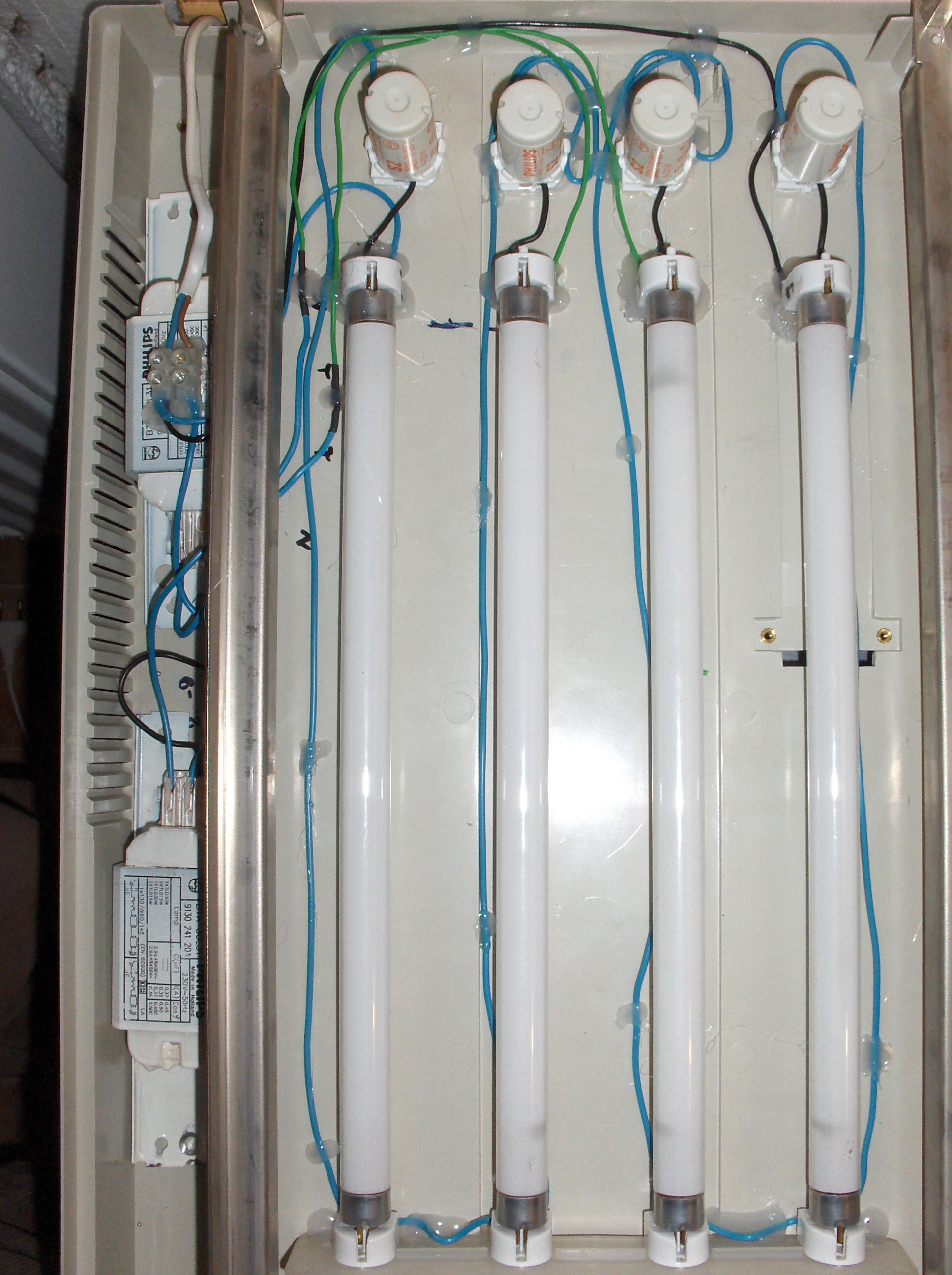
Manufacturing circuitboards containing SMD-parts with toner-transfer is nearly impossible. The thin traces almost never get transferred completely to the copper. One solution to this problem is to use photoresist boards and expose them with UV light.
The layout is printed onto a transparency, which is then used as a mask for the photoresist. I got the best results with inkjet-printed layouts. They seem to be more opaque than laserprinted ones.The cheapest UV exposure unit from Reichelt costs 200€. That’s far too much for what is essentially some UV-light source and a glassplate.
A much cheaper way to get one, is to build it yourself.
So i got a broken scanner (the older, the better (bigger housing)) and a face tanner (not broken, but old) from eBay. The tanner contained 4 UV tubes, 2 trafos and 4 starters. All this was glued into the gutted scanner with hot glue. About 90 seconds per layout seem to sufice for good exposure. The boards are then developed in a 10% sodiumhydroxide solution and etched in a mixture of hydrochloric acid and hydrogen peroxide. (More information on this etching solution in this great tutorial). The remaining photoresist can be removed with isopropanol. For more Detail: UV Exposure Unit & Etching

